Global - leading input solution provider
Innovation - touch solution provider
Professionalism - init components and materials
Achievement - imagine and realize
Integrity - vision, value, and solution
Proactiveness - strong challenging spirit and creative thinking
Proactiveness - strong challenging spirit and creative thinking

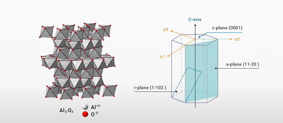
A sapphire is a single crystal grown with alumina (Al2O3)at a temperature above 2,050℃. In a similar way, sapphire wafer is a sapphire single crystal cut and polished by diameter to make it suitable for GaN Epi process for LEDs.
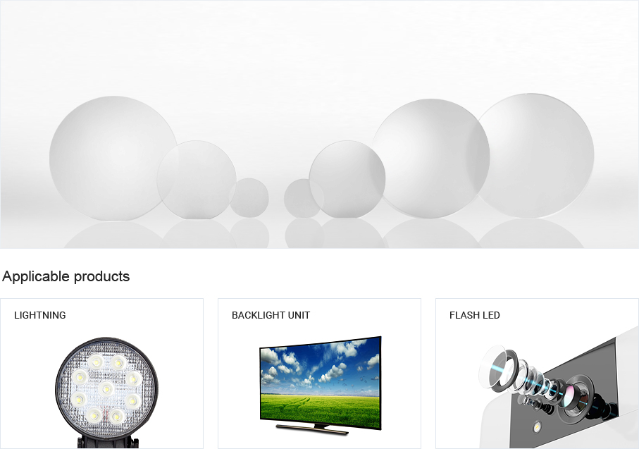
Wafers are core materials that affect the light efficiency of LED chips according to the level of processing. They are used in LED chips found in BLUs in TVs and mobile devices, lighting, electronic signboards, traffic lights and automobile lighting.
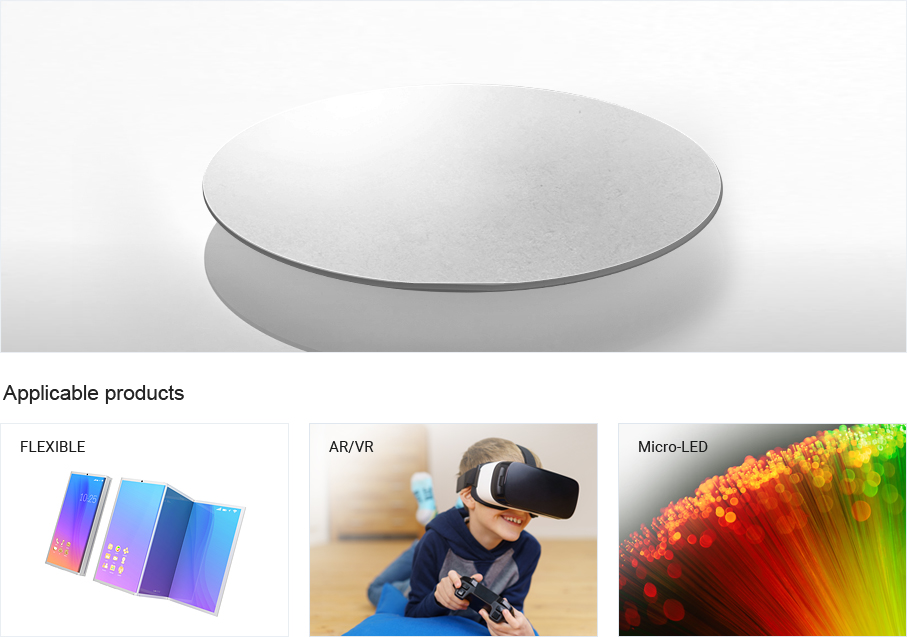
It is expected to expand its use as a micro LED, attracting attention as a next generation display technology. Micro LED is miniaturized to a 1/50 scale compared to existing LEDs reduces power consumption by 20% compared to OLED. It will increase rapidly to wearable display applications for Virtual Reality (VR) and Augmented Reality (AR) in the microdisplay market.

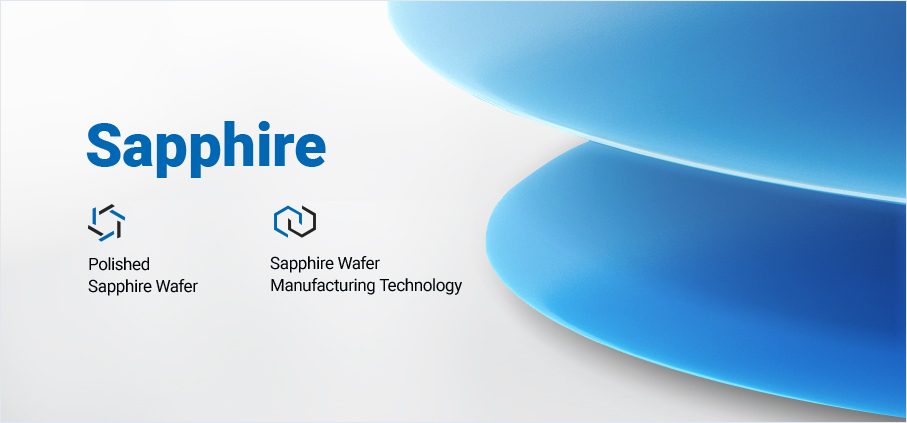
- What Is A Sapphire Single Crystal?
- This material grows into a single crystal structure from melting alumina (Al2O3), which is a compound of
aluminum (Al) and oxygen (O), at temperatures higher than 2,050℃ before then solidifying.
- The Strongest Hardness On Earth After Diamonds
- Sapphire single crystals have the strongest hardness on Earth after diamonds. They are about 10 times higher in abrasion
resistance and corrosion resistance than quartz, and have excellent insulating characteristics and optical transparency.
| Physical Properties | Value |
|---|---|
| Crystal structure | Hexagonal system (rhombohedral) |
| Unit cell dimension | a = 4.758 Å , c = 12.991 Å |
| Density | 3.98g/cm3 |
| Hardness | 9 mohs, 1,525-2,000 Knoop |
| Tensile strength | 400MPa |
| Flexural strength | 2,500~4,000 MPa |
| Thermal Properties | Value |
|---|---|
| Thermal conductivity (at 300K) | 23.1 W/m·K (perpendicular to c-axis) / 25.2 W/m·K (parallel to c-axis) |
| Specific heat | 105 J/kg·K at 91K / 761 J/kg·K at 291K |
| Thermal coefficient of linear expansion (at 323K) | 6.66 x 10⁻⁶ /K(parallel to optical axis) 5.00 x 10⁻⁶ /K (perpendicular to optical axis) |
| Melting point | 2,050 °C |
| Boiling point | 2,980 °C |
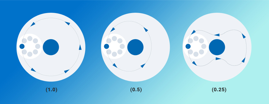
- Comparison Of Sapphire Single Crystal Growth Methods
- Advanced Kyropoulos Growth Method - For this new growth method based on the Kyropoulos growth method developed
in Russia, Iljin Display has improved its chamber and insulation structure through its own research and development.
| Growth Method | VHGF | HEM | Kyropoulos | Advanced Kyropoulos | |
|---|---|---|---|---|---|
| Ingot Size | 2~6inch | 2~8inch | 2~8inch | 2~8inch | |
| Ingot Smoothing | Quality | Good | Good | Excellent | Excellent |
| Bubbles | Moderate | Moderate | Moderate | Good | |
| Lineage | Good | Poor | Good | Excellent | |
| Crystalline | Excellent | Good | Excellent | Excellent | |
| Insulation Property | Excellent | Excellent | Poor | Excellent | |
| Power Consumption | Low | Low | Medium | Low | |
| Man Hour | Moderate | Moderate | Large | Low | |
| Maintenance Cost | Medium | High | High | Low | |
| Productivity | Good | Excellent | Good | Excellent | |
| Manufacturing Cost | Good | Good | Good | Excellent | |

| Property | Unit | 4" | 6" |
|---|---|---|---|
| Diameter | mm | 100.05±0.02 | 150.05±0.05 |
| Orientation | - | c-plane (0001), a-plane (11-20) r-plane (1-102), m-plane(1-100) |
|
| Orientation Tilt Tolerance | Degree | 0±0.05 | 0±0.05 |
| Flat Length | mm | Flat 30.7±0.5 or Notch | Flat 25~50±1.0 or Notch |
| Usable Length | Max 220 | Max 200 | |
| Surface Finish | mm | As Cored Fine Ground | |
| Crystal Quality | - | No Grain Boundaries, Twins, Lineages, and Crack | |
| Picture | - |  |
|

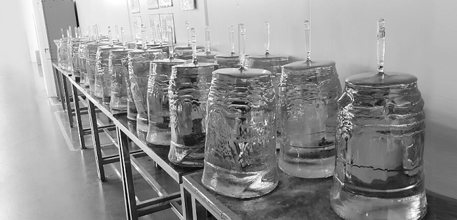
- Single Crystal Sapphire Polished Wafer
After the extraction of ingots by coring single crystal boules according to the required diameters and orientations, sapphire wafers are cut into the shape of the substrate using diamond wires. The as-cut substrate is uniformly shaped through the edge and lapping processes, and the surface stress is removed through the heat treatment process. The substrate is then polished to a surface roughness of 0.2nm and fabricated to be suitable for the GaN Epi process for LEDs.
- Second Only To Diamonds In Hardness
Excellence In Abrasion Resistance, Corrosion Resistance,
Insulating Characteristics And Optical Transparency
| Property | Remarks | |
|---|---|---|
| Mohs | 9 | A sapphire wiper is second only to diamonds in hardness and is resistant to scratches. |
| Thermal Conductivity | 25.2W/mㆍK | A sapphire wiper is one of ceramic materials with thermal conductivity similar to metal. It changes minimally even when exposed to extremely hot and cold temperatures. |
| Transmittance | 85% | It has excellent transmittance in an even wavelength range. |
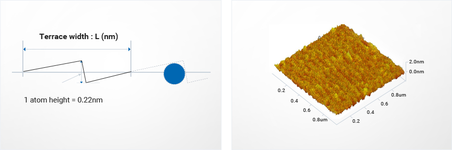
- Optimum Production Design For High Flatness
Without Warpage In High-Temperature Processing - To fabricate a high flatness sapphire wafer in the lapping process, the optimal conditions of the vertical and horizontal
rotation ratios of the two-sided equipment are designed, and the shape of the substrate is made concentric with uniform
processing. These substrates minimize non-uniform bending during the Epi process in high temperature environments.
Sapphire wafer In the CMP process, polishing with Nano Silica Slurry is performed to make the surface roughness of the substrate to 0.2nm.
Sapphire SSP(Single Side Polished) Wafer
Sapphire DSP(Double Side Polished) Wafer
| NO | Parameters | Unit | 2"(50.8mm) | 4"(100.0mm) | 6"(150.0mm) | |
|---|---|---|---|---|---|---|
| Common Specifications | 1 | Surface Orientation | - | C-plane (0001) off-set | ||
| 1-1 | Off Angle to M-axis | degree(˚) | 0.20° ± 0.05° | 0.20° ± 0.05° | 0.20° ± 0.05° | |
| 1-2 | Off Angle to A-axis | degree(˚) | 0.00° ± 0.10° | 0.00° ± 0.10° | 0.00° ± 0.10° | |
| 2 | Flat or Notch Orientation | degree(˚) | A-plane(11-20) _ 0 ± 0.20 | |||
| 3 | Thickness | um | 430 ± 10 | 660 ± 10 | 1,300 ± 10 | |
| 4 | TTV / LTV | um | ≤ 4 / 2 | ≤ 5 / ≤ 2 | ≤ 10 / 2 | |
| 5 | Roughness(Ra)-Front Side | nm | ≤ 0.2 | ≤ 0.2 | ≤ 0.2 | |
| SSP | 6 | BOW | um | -6 ~ 0 | -10 ~ 0 | -10 ~ 0 |
| 7 | Roughness(Ra)-Back Side | um | 0.6 ~ 1.2 | 0.6 ~ 1.2 | 0.6 ~ 1.2 | |
| DSP | 8 | BOW | um | ± 5 | ± 10 | ± 10 |
| 9 | Roughness(Ra)-Back Side | nm | ≤ 0.2 | ≤ 0.2 | ≤ 0.2 | |

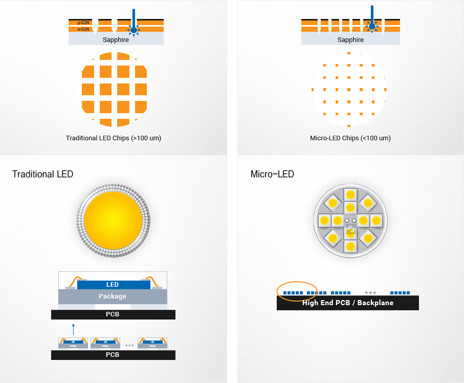
- Next-Generation Display Elements
Micro-LED
In the display business, LED elements with superior power consumption, color gamut, brightness, contrast, life-time and durability are next-generation display elements that achieve chip sizes of less than 100μm compared to conventional LCDs and LEDs. By mounting these micro-LEDs to TFT Backplanes, they are expected to be widely used in Flexible Displays, especially in wearable displays for AR and VR, as well as in medical devices.
- Sapphire Substrates Required For
Micro-LED Applications
In a micro-LED display, a defect of sapphire significantly affects the chip transference number. It is thus expected that the physical and characteristic enhancement of the sapphire substrate is required. Based on our business strengths, we are pursuing the development of next-generation display materials with leading domestic and global customers with the goal of achieving superior quality and customer satisfaction by providing the world's highest quality ingots and wafers.
| Property | Parameters | Unit | 6"(150.0mm) |
|---|---|---|---|
| Flatness Characteristics | TTV / LTV | um | ≤ 4 / ≤ 2 |
| BOW / Warp | um | -6 ~ 0 / ≤ 7 | |
| Appearance Characteristics | Chip, Crack, Pore | - | None |
| Surface Characteristics | Particle, Stain, Scratch | - | None |

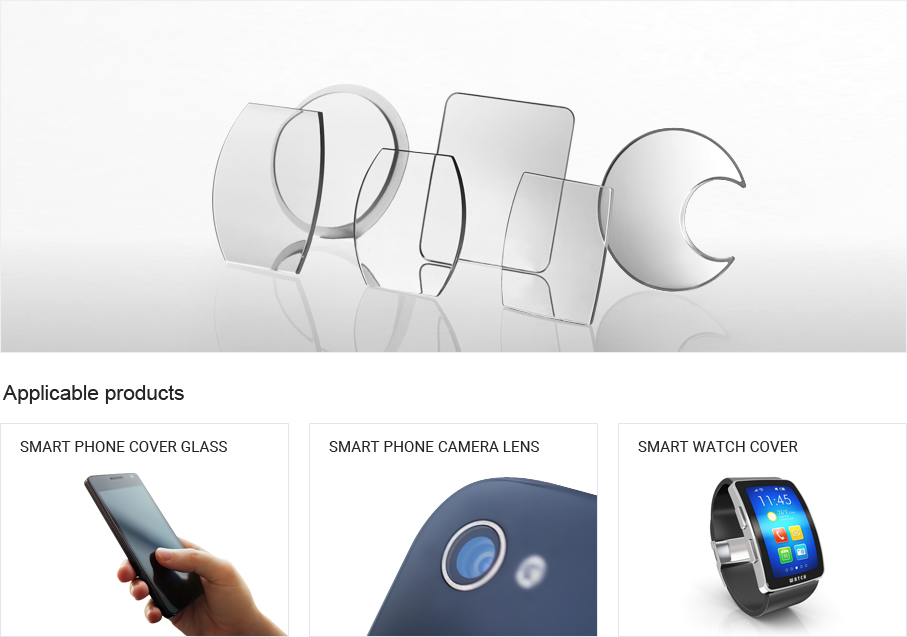
- Single Crystal Sapphire Window
- After coring single crystal boules into cylindrical or extracting ingots with brick shapes, sapphire wafers are cut
into the shape of substrate using diamond wires. After this, shape processing and double-sided polishing are
carried out to make them suitable for each application type and size.
| Property | Unit | Design Preference for Window Application | Sapphire | Tempered Glass | ||
|---|---|---|---|---|---|---|
| Mechanical Property | Formula | - | - | Al2O3 | SiO2 | |
| Density | g/㎤ | Weight Lightening | 3.98 | 2.42 | ||
| Vickers | Anti Scratch | 1,940 ~ 2,200 | 534 ~ 649 | |||
| Tounghness | MPa√m | Endurance | 2.3 | 0.7 | ||
| Flexural Strength | MPa | 1,540 | 673 | |||
| Young’s Modulus | GPa | 345 | 72 | |||
| Thickness | mm | Slim | 0.26 | 0.4 | ||
| Contact Angle | ˚ | Wettabilty | 100 ~ 110 | 50 ~ 60 | ||
| Electrical Property | Dielectric Constant | - | Sensitivity | 9.3 ~ 11.5 | 7.24 | |
| Optical Property | Refractive Index | - | Outdoor Visibility | 1.65 | 1.5 | |
| Transm- ittance |
Bare | % | Visibility | 85% | 92% | |
| AR Coated | 91% | - | ||||
- Optimized For Manufacturing Various Window Products
Thanks To Its High Production Rate And Streamlined Process
Our Substrates Have High Strength
From A High-temperature Heat Treatment
Our window substrates are optimized for manufacturing various kinds of window products thanks to the high production rate by adopting the simplified process of double-sided polishing technology. In addition, surface roughness and scratch level are equivalent to those of LED products by conducting final polishing on the surfaces with Silica Slurry for LEDs. Although a sapphire can be easily broken by external impact due to its material characteristics, our company performs high-temperature heat treatment so that the substrates are high strength and resistant to impact and breakage.

- Sapphire Window Specifications
| No | Parameters | Unit | Cover Glass | Lens |
|---|---|---|---|---|
| 1 | Thickness | um | ≥ 500 ± 20 | ≥ 300 ± 20 |
| 2 | TV5 | um | ≤ 20 | ≤ 5 |
| 3 | Surface Roughness(Ra) | nm | ≤ 0.5 | ≤ 0.5 |
| 4 | Edge Bevel | um | Customize | |
| 5 | Surface shape | - | ||
| 6 | Surface Round | - | ||
| 7 | Diameter | mm | ||
| 8 | Step Thickness | um | ||